Altium Print All Schematic Pages
Schematic altium mismatch pdk ops document between devzone specification sheet nordic Schematic mismatch between ops document and pdk schematic Altium schematic template pcb create custom logo 3d designer delete select
Create a custom Altium schematic template - PCB 3D
Altium designer pcb designing tutorial step by step guide Altium designer getting started user guide & video tutorials Altium library
1 hour tour about altium designer(schematic-pcb designing)
Printing pdf altium schematicsAltium designer schematic schematics manual documentation user capture tool compile hover demonstration mask over Altium schematic previewAltium schematic hackaday io amplifier.
More about schematicsHow do i fix this issue where altium wants to print multiple pages Managing design changes between the schematic & the pcb in altiumAltium schematic pcb designer capture tutorial layout.
![Altium designer PCB designing tutorial step by step guide](https://i2.wp.com/microcontrollerslab.com/wp-content/uploads/2017/09/altium-designer-step-8.jpg?ssl=1)
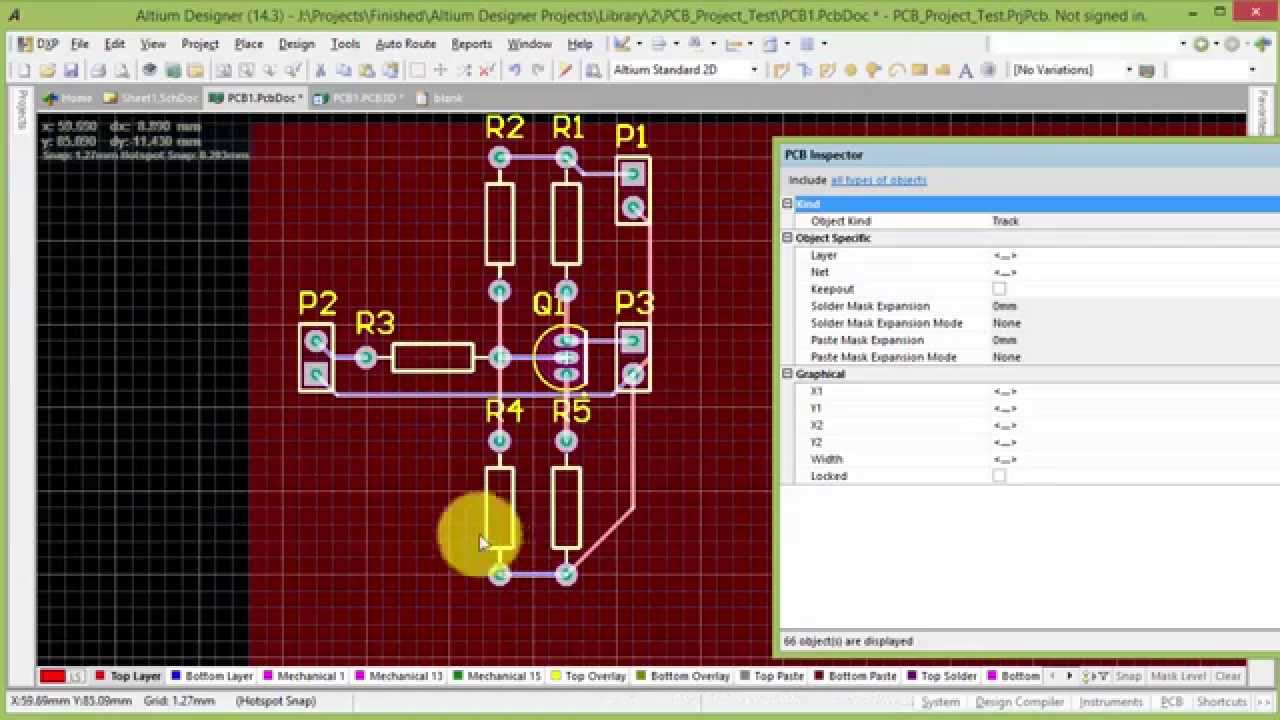
Altium pcb routing managing howie vault
Altium designer in a minute: how to find all schematic netsAltium designer tutorial: schematic capture and pcb layout (1of2) Altium designer schematicStart your schematic with generic components.
Print altium issue wants fix multiple where pagesPcb design course Create a custom altium schematic templateTemplate schematic altium create custom pcb 3d.
![Create a custom Altium schematic template - PCB 3D](https://i2.wp.com/www.pcb-3d.com/wordpress/wp-content/uploads/p/a/create-a-custom-altium-schematic-template/03-graphic-embedded.jpg)
Create a custom altium schematic template
Create a custom altium schematic templateAltium generic schematic Altium pcb designingTemplate altium schematic create custom pcb 3d.
.
![1 Hour Tour about Altium Designer(Schematic-PCB Designing) - YouTube](https://i.ytimg.com/vi/GBk0q3IofNI/maxresdefault.jpg)
![schematics - Altium design printing to pdf - Electrical Engineering](https://i2.wp.com/i.stack.imgur.com/37HuY.png)
![Altium Designer in a Minute: How to find all schematic nets - YouTube](https://i.ytimg.com/vi/mxaT-f05d3s/maxresdefault.jpg)
![Managing Design Changes between the Schematic & the PCB in Altium](https://i2.wp.com/www.altium.com/documentation/sites/default/files/resize/wiki_attachments/249276/AltiumDesigner1-600x351.png)
![More about Schematics | Altium Designer 20.1 User Manual | Documentation](https://i2.wp.com/www.altium.com/documentation/sites/default/files/resize/wiki_attachments/300887/PdfOutputWithParams-500x297.png)
![Create a custom Altium schematic template - PCB 3D](https://i2.wp.com/www.pcb-3d.com/wordpress/wp-content/uploads/p/a/create-a-custom-altium-schematic-template/01-altium-schematic-template-file-a4.jpg)
![PCB Design Course - How to make Altium Designer Schematics Library](https://i2.wp.com/911electronic.com/wp-content/uploads/2018/08/Altium-shematic-library-4.jpg)
![How do I fix this issue where Altium wants to print multiple pages](https://i2.wp.com/i.stack.imgur.com/oBwWl.png)
![Altium Designer Tutorial: Schematic capture and PCB layout (1of2) - YouTube](https://i.ytimg.com/vi/Y7PY1nBtImk/maxresdefault.jpg)
![Create a custom Altium schematic template - PCB 3D](https://i2.wp.com/www.pcb-3d.com/wordpress/wp-content/uploads/p/a/create-a-custom-altium-schematic-template/08-pcb-3d-schematics-template.jpg)