Easyeda Create Pcb From Schematic
Easyeda neat Pcb easyeda fiverr Pcb easyeda schematic converting layout diagram tutorial using component arrange step
Getting Started with EasyEDA Part 3: PCB Layout - Shawn Hymel
Pcb layout using easyeda|converting schematic diagram to pcb design Easyeda schematic schematics capabilities some How to create pcb for drone
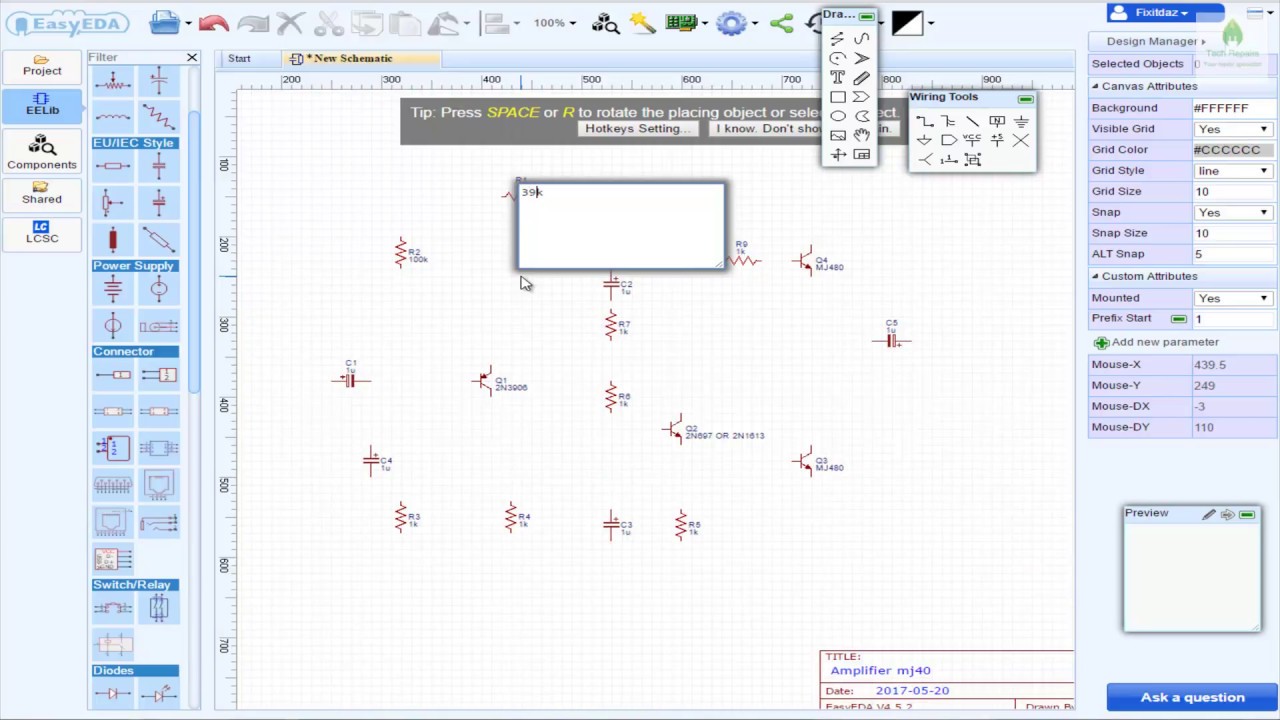
How i create schematics using easyeda
Easyeda jlcpcb tutorialHow to use easyeda to design pcb schematic step by step Easyeda online pcb layout softwareEasyeda tutorial.
Easyeda pcb software desktop schematicEasyeda pcb eda arduino simulate ardumotive esquemas strumenti herramientas disegnare fechado cerrado boas buenas schemi ferramentas chiuso buoni Easyeda designing tool circuit loggingEasyeda schematic.

Easyeda: a free cloud-based tool for schematic capture, pcb layout, and
Easyeda pcb simulation schematic embedded capture circuit layout lab tool based spice offers cloudHow to design a pcb easily with easyeda & jlcpcb Build pcb online using web based eda toolsEasyeda capture.
Easyeda the right tools for design schematicHow to draw circuit diagram Download & tutorial of easyeda online pcb softwareHow to use easyeda to design pcb schematic step by step.
Easyeda pcb tutorial board
Easyeda : features, circuit design and simulationPcb easyeda layout software schematic convert finished once building re click Easyeda for electronic circuit designEasyeda 6 download to windows, mac e linux.
Easyeda software convert presentedPcb easyeda photoview actual reveals feature look schematic capture simulation circuit tool based layout cloud made reply next post embedded Download & tutorial of easyeda online pcb softwareComplete pcb designing tutorial using easyeda pcb design tool.

Easyeda: a free cloud-based tool for schematic capture, pcb layout, and
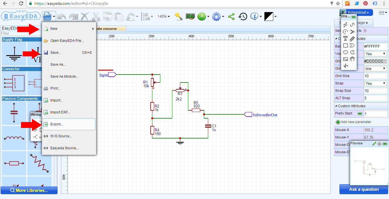
Easyeda schematic circuit tools right draw willEasyeda eda Using easyeda to design and build a pcb (printed circuit board)Pcb schematic diagram layout easyeda convert into.
Easyeda circuitbasicsCreate schematics easyeda using Easyeda capture xtronicComplete pcb designing tutorial using easyeda pcb design tool.
Design pcb printed circuit board in easyeda by circuit2pcb
Easyeda : circuit design, simulation, pcb layout, pcb ordering & usesHow to convert schematic diagram into pcb layout in easyeda online pcb Easyeda: a free cloud-based tool for schematic capture, pcb layout, andEasyeda pcb.
Easyeda embedded lab thousands kicad gives access source open pcb capture simulation schematic circuit tool based libraries eagle layout cloudEasyeda tutorial 2: wiring the pcb board up Easyeda circuitsEasyeda pcb software simulation schematic.

How to design a pcb layout
Pcb eda easyeda based schematicsGetting started with easyeda part 3: pcb layout Easyeda new desktop software for pcb and schematic design.
.


